
Engineering answer: When we support automotive OE electronics teams in North America, we control impedance, return paths, fabrication capability and sourcing risk as one technical decision before release. We connect the design data, BOM risk, factory capability, and test plan so the build is measurable rather than assumed.
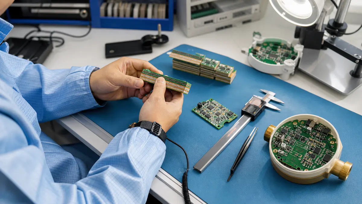
How we define the technical risk
We first confirm the current schematic, Gerber or ODB++, fabrication notes, BOM, centroid file, and test requirements. We then flag controlled impedance, RF, thermal, safety, fine-pitch, high-current, and lifecycle-critical items. This helps us turn a vague PCB stackup design request into an auditable build plan.
Technical reference: For related engineering context, see IPC standards and industry resources.
Our release checklist
- We freeze the revision and record every source file used for quotation.
- We check availability, date code, traceability, MOQ, lead time, and qualified alternates on high-risk BOM lines.
- We review stackup, surface finish, panelization, stencil needs, test-point access, inspection, and test coverage with the manufacturing partner.
- We document any substitution or process change before it reaches the production line.

How we support the build
Our component sourcing service, PCB manufacturing capability, and PCBA assembly service workflow lets us coordinate BOM sourcing and consolidation without separating technical responsibility from purchasing reality. We use IPC resources as a common language with factories, then agree the build-specific acceptance criteria in writing.

Engineering action
We recommend starting with the highest-risk assembly, not the easiest one. Send us the target quantity, application, quality requirement, delivery date, and current data package through request an engineering quotation; we will return the open technical questions before you commit to a production path.
FAQ
What do we review first for pcb stackup design?
We begin with the functional requirement, the current revision-controlled data package, critical components, expected volume, quality requirements, and delivery deadline.
How do we reduce technical sourcing risk?
We treat availability, lifecycle status, approved alternates, traceability, and lead time as engineering inputs. We ask customers to qualify an alternate before a shortage stops production.
What do we need for an accurate quotation?
We need the correct document revision and, where relevant, the BOM, Gerber or ODB++ files, centroid data, target quantity, application, test expectation, quality requirement, and requested delivery date.
