
When we review a smart water meter PCBA layout, the first question we ask is not about data rates or communication protocols. It is about where the heat goes. For a device sealed in a brass or polymer housing, buried in a pit or mounted on a wall, there is no fan, no heat sink airflow, and often no easy way to measure junction temperature after final assembly. The power electronics. the switching regulator, the battery-charge path, the motor-drive FETs for the shut-off valve. can generate enough heat to shift a 100 ppm/°C reference voltage or push an MCU into thermal shutdown. We have seen designs that work perfectly on the bench and fail in the field because the thermal path was an afterthought. This article is our working checklist for thermal management in smart water meter power electronics, written from the perspective of the engineers who source the BOM and review the DFM.
Start with a Direct Answer: What Does Thermal Management Mean for This Product?
For a smart water meter, thermal management is not about exotic cooling. It is about predicting the worst-case ambient temperature, the self-heating of the power stage, and the thermal resistance from the junction to the outside world, then verifying that the maximum junction temperature stays below the derating curve for every component. The practical goal is to keep the PCB temperature rise below 20 °C above ambient at maximum continuous load, and below 10 °C for the battery-charging circuit. If you cannot guarantee that, you need to change the layout, the component package, or the heat-spreading copper area before you commit to a BOM.
Technical reference: For related engineering context, see IPC standards and industry resources.
We use a three-step engineering flow: define the thermal budget, select components with the right thermal metrics, and verify with a board-level review. This is not a simulation-heavy process for every project, but it is a discipline that prevents re-spins.
Step 1: Define the Thermal Budget Before You Choose a Regulator
We ask the design engineer for three numbers: maximum ambient temperature in the meter pit (typically 55 °C for buried installations in the southern US, but we have seen 70 °C in direct sunlight), the maximum continuous current draw from the power rail (often 50 mA for a LoRa radio in transmit, but the valve actuator can pull 500 mA for 2 seconds), and the allowable PCB temperature rise. With those numbers, we can calculate the maximum allowable power dissipation for the linear regulator or the efficiency requirement for the buck converter.
For example, if you have a 24 V input, a 3.3 V output, and 50 mA continuous load, a linear regulator dissipates about 1 W. In a sealed enclosure, that is a lot. A buck converter at 85% efficiency dissipates only 30 mW for the same output. The component selection is not only about cost; it is about whether the package can move that heat to the PCB. We always ask: Is the thermal pad on the regulator connected to a copper pour that extends to the edge of the board? If not, the thermal resistance from junction to ambient (RθJA) will be higher than the datasheet value, which is measured on a 2-layer board with a specific copper area.
Thermal Metrics We Read in Datasheets
We do not rely on the single RθJA number. We look for the thermal resistance from junction to case (RθJC) and from junction to PCB (RθJB). For a DFN or QFN package, RθJB is the number that matters because the heat flows through the solder to the PCB. For a SOT-23, RθJA is more relevant because the heat flows through the leads. We also check the thermal derating curve. the graph that shows maximum current vs. ambient temperature. If the curve drops sharply above 50 °C, the part is not suitable for a meter pit in Arizona.
Here is a practical table we use when reviewing a proposed BOM for the power stage:
| Component | Key Thermal Metric | Our Review Question | Acceptable Range for Meter |
|---|---|---|---|
| Buck converter IC | RθJB (junction-to-board) | Is the thermal pad exposed and connected to a 1 oz or 2 oz copper pour? | RθJB < 20 °C/W |
| MOSFET (valve driver) | RθJC (junction-to-case) | Can the case dissipate 1 W peak without exceeding 125 °C junction? | RθJC < 10 °C/W |
| Battery charger IC | Power dissipation at max charge current | Does the package have a thermal pad or is it a leaded package? | Dissipation < 0.5 W continuous |
| Sense resistor | Temperature coefficient and self-heating | At 500 mA, does the resistor heat up more than 5 °C? | Power rating > 2x actual |
We use this table in every BOM review. It forces a conversation about the physical package, not only the electrical specs.
Step 2: Layout Rules We Enforce in the DFM Review
When we receive the Gerber files for a smart water meter PCBA, we look for specific thermal features. We do not only check for electrical connectivity. Here is our DFM thermal checklist:
- Copper thickness: We recommend 2 oz copper for the power section, even if the rest of the board is 1 oz. The extra 35 µm of copper reduces spreading resistance by half.
- Thermal vias: For a QFN package, we require at least 4 thermal vias under the exposed pad, each with a 0.3 mm drill size and filled with solder or epoxy. Unfilled vias wick solder away and create voids.
- Copper pour continuity: The pour under the regulator must extend at least 5 mm in all directions, with no slots or cuts that interrupt the heat path. We have seen designs where a routing channel cut through the pour and raised the junction temperature by 15 °C.
- Component placement: The valve driver FETs should be placed near the edge of the board, away from the MCU and the radio. We also ask for a 3 mm keep-out zone around the FETs to allow for heat spreading to the housing wall if a thermal pad is used.
- Thermal interface material (TIM): If the meter housing has a metal insert, we recommend a 0.5 mm gap pad between the FET case and the housing. This is not always specified in the original design, but we flag it as a DFM suggestion.
We also ask a simple question: Where is the antenna, and where is the power stage? If the radio is on the same edge as the FETs, the radiated heat can shift the RF oscillator frequency. We prefer to separate the two by at least 10 mm of ground copper.
Figure 1: Typical Power Stage Layout with Thermal Vias and Copper Pour
Step 3: BOM Sourcing with Thermal Risk in Mind
We source components for smart water meter PCBA builds every week. The thermal performance of a part can vary by manufacturer and by lot. We do not only check the part number; we check the package version. A buck converter in a SOT-23-6 will have a different RθJA than the same die in a DFN-8. We ask the distributor for the exact package code and the thermal data sheet revision.
We also consolidate the BOM to reduce the number of unique packages. If we can use one DFN-8 package for both the buck converter and the battery charger, we reduce the number of stencil apertures and the risk of solder voids. Fewer unique thermal pads mean fewer places where heat transfer can fail. This is a sourcing strategy, not only a cost-saving measure.
When we send a quote request to our suppliers, we include a note about the thermal requirements. We specify the maximum junction temperature and the expected copper area on the PCB. This helps the distributor recommend an alternate part if the original is on long lead time. We have seen many cases where a distributor suggests a pin-compatible part with a worse thermal package. the RθJA is 20% higher, but the price is lower. We reject that substitution unless the design engineer approves the thermal impact.
Figure 2: Thermal Resistance Comparison for Common Power Packages

RFQ and DFM Steps We Recommend for Your Next Project
When you are ready to move from schematic to prototype, here is the sequence we follow with our pcbManufacturing partner:
- Send the thermal budget in the RFQ: State the maximum ambient temperature, the maximum continuous current, and the allowed junction temperature. This is not a standard RFQ field, but we include it in the notes.
- Request a thermal simulation for the power stage: Most PCB manufacturers can run a simple steady-state thermal analysis if you provide the copper area and the component power dissipation. This costs a few hundred dollars and can prevent a re-spin.
- Review the stencil design for the thermal pad: We ask for a 50% coverage of the thermal pad with solder paste. Too much paste creates voids; too little creates a poor thermal connection. Our pcba team has a specific stencil aperture design for DFN and QFN packages.
- Build a thermal test coupon: On the same panel as the production board, we add a small coupon with a resistor and a thermocouple pad. This lets us measure the actual board temperature rise during the first article test.
We also recommend a simple field test: place the prototype meter in a thermal chamber set to 55 °C, run the valve actuation cycle 100 times, and measure the case temperature with a thermocouple. If the case temperature exceeds 85 °C, the thermal path is insufficient. This is a pass/fail test that does not require simulation.
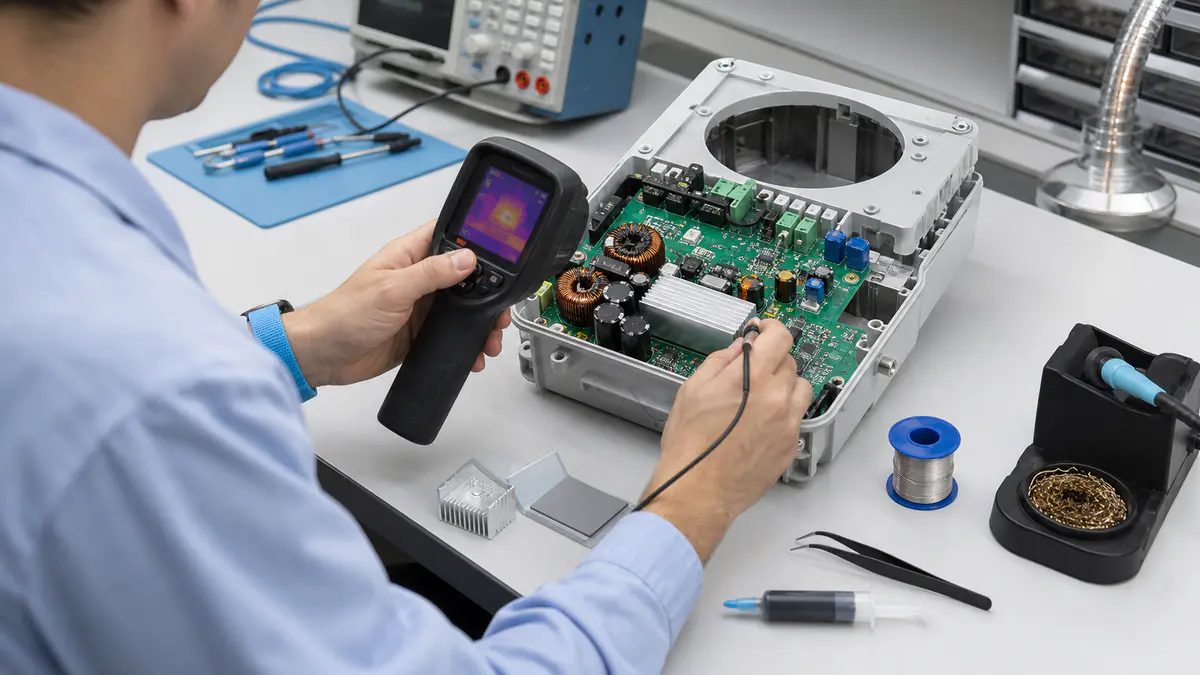
Figure 3: Thermal Camera Image of a Smart Water Meter PCBA Under Load

FAQ: Thermal Management for Power Electronics in Smart Water Meters
Q1: What is the maximum junction temperature we should allow for a smart water meter power IC?
We use 125 °C as the absolute maximum for silicon, but we design to a target of 105 °C at the worst-case ambient. This gives a 20 °C margin for aging, solder void formation, and part-to-part variation. For the battery charger IC, we use a lower target of 95 °C because the charge current accuracy degrades with temperature. Check the derating curve in the datasheet. many parts specify a 50% current reduction above 85 °C ambient.
Q2: How many thermal vias should we place under a QFN package?
We recommend a minimum of 4 vias, but the exact number depends on the via size and the copper thickness. For a 0.3 mm drill, we use 4 to 9 vias in a grid pattern. The vias must be filled with non-conductive epoxy or solder to prevent solder wicking. If the vias are not filled, the solder paste will flow into the holes and create voids under the thermal pad, which increases RθJB by 30% or more. We specify filled vias in our DFM notes.
Q3: Can we use a linear regulator if the input voltage is high and the current is low?
It depends on the power dissipation. For a 24 V input and a 3.3 V output at 10 mA, the dissipation is 0.21 W. In a sealed enclosure, that is acceptable if the PCB has a copper pour of at least 1 cm². But if the current is 50 mA, the dissipation is 1 W, which will raise the junction temperature by 50 °C to 80 °C depending on the package. We would not approve a linear regulator for that case. A buck converter is the safer choice, even if it costs a few cents more. We always run the numbers before we recommend a part.
For any new design, we are happy to review your schematic and layout for thermal risks. Send us your BOM and a note about your operating environment, and we will provide a DFM review with specific thermal recommendations. The goal is to get the heat out before you commit to a production run.
FAQ
What do we review first for thermal management for power electronics?
We begin with the functional requirement, the current revision-controlled data package, critical components, expected volume, quality requirements, and delivery deadline.
How do we reduce technical sourcing risk?
We treat availability, lifecycle status, approved alternates, traceability, and lead time as engineering inputs. We ask customers to qualify an alternate before a shortage stops production.
What do we need for an accurate quotation?
We need the correct document revision and, where relevant, the BOM, Gerber or ODB++ files, centroid data, target quantity, application, test expectation, quality requirement, and requested delivery date.
