
0402 vs 0603 vs 0805: SMD Package Size Selection Strategy for PCB Design
Selecting the right SMD (Surface-Mount Device) package size is one of the earliest and most consequential decisions in PCB design. The choice between 0402, 0603, and 0805 packages ripples through every stage of the product lifecycle — from schematic capture and layout to assembly yield, thermal performance, and field reliability. Yet many engineers default to "what we used last time" without a structured evaluation.
This article provides a comprehensive, data-driven framework for selecting between 0402, 0603, and 0805 passive component packages. We cover dimensional specifications, electrical performance (ESL, power rating), mechanical reliability (tombstoning, MLCC cracking), cost trends, manufacturability, and application-specific recommendations across mobile, industrial, automotive, and military domains.
1. Dimensional Specifications: What the Numbers Mean
SMD package designations are derived from imperial dimensions. The first two digits represent length, the last two represent width — both in hundredths of an inch.
| Package | Length (inches) | Width (inches) | Length (mm) | Width (mm) | Typical Height (mm) |
|---|---|---|---|---|---|
| **0402** | 0.04″ | 0.02″ | 1.0 | 0.5 | 0.35–0.50 |
| **0603** | 0.06″ | 0.03″ | 1.6 | 0.8 | 0.45–0.80 |
| **0805** | 0.08″ | 0.05″ | 2.0 | 1.2 | 0.55–1.25 |

The area footprint difference is dramatic: an 0805 occupies approximately 4.8× the board area of an 0402 (2.0 × 1.2 mm vs. 1.0 × 0.5 mm). This has immediate implications for board density, especially in designs where passives can number in the hundreds [1].
Metric vs. Imperial Confusion: A common pitfall for engineers working with international suppliers is the metric naming convention. A metric 0402 (0.4 mm × 0.2 mm, also called 01005 imperial) is vastly smaller than an imperial 0402. Always verify which standard your BOM or datasheet uses. Throughout this article, all references are to imperial sizing unless stated otherwise [2].
2. 0402: The Miniaturization Champion
The 0402 package is the de facto standard for high-density consumer electronics. Its small footprint enables slimmer end products and shorter trace lengths — both critical in modern designs.
2.1 Advantages
Lowest ESL (Equivalent Series Inductance). Smaller physical dimensions mean shorter internal electrode paths, which directly translates to lower parasitic inductance. For decoupling capacitors in high-speed digital circuits (DDR memory rails, FPGA core supplies, RF power amplifiers), an 0402 MLCC typically exhibits ESL in the 0.2–0.4 nH range, compared to 0.4–0.6 nH for 0603 and 0.6–0.9 nH for 0805 [3]. This makes 0402 the preferred choice when PDN (Power Distribution Network) impedance targets are tight.
Superior MLCC Crack Resistance. This is counterintuitive but well-documented: smaller ceramic capacitors are mechanically more robust against board flexure. According to the IPC/JEDEC-9704 guidelines, an 0402 MLCC can withstand approximately 2× the board strain of an equivalent 0805 before cracking, because the bending moment applied across a shorter component body is proportionally smaller [4]. For designs subject to mechanical stress — drop-prone handheld devices, vibration-heavy environments — 0402 actually offers better reliability.
Maximum Board Density. When a smartphone PCB must accommodate 300+ passives alongside an application processor, PMIC, and multiple radio chains, every square millimeter matters. Switching from 0805 to 0402 for bypass capacitors alone can reclaim 30–50% of the passive-component board area.
2.2 Disadvantages
Hand-Soldering Difficulty. An 0402 component is smaller than a grain of pepper. Hand-soldering under a microscope requires steady hands, fine-tipped soldering irons, and considerable practice. For prototyping and low-volume production, this adds time and defect risk.
Tombstoning Susceptibility. Tombstoning — where one end of a passive lifts off the pad during reflow — is more prevalent with smaller packages. The reduced thermal mass of 0402 means uneven heating across the two terminations is more likely. Mitigation strategies include symmetrical pad design, optimized stencil aperture geometry, and nitrogen-atmosphere reflow to improve wetting uniformity [5].
Lower Power Handling. The maximum power rating for an 0402 thick-film resistor typically caps at 1/16 W (0.063 W), limiting its use to signal-level circuits. For current-sensing or power-supply divider applications, larger packages are necessary.
PCB Fabrication Requirements. Reliable 0402 assembly demands tighter PCB manufacturing tolerances: solder mask registration ≤ 50 μm, pad-to-pad spacing ≥ 0.15 mm, and typically ENIG or OSP surface finish for consistent solderability. These requirements are standard for volume manufacturers but may exclude low-cost prototype shops.
3. 0603: The Balanced Workhorse
If 0402 represents the cutting edge of miniaturization and 0805 represents traditional robustness, the 0603 package occupies the pragmatic middle ground. It is the most widely used passive package size across all electronics sectors.
3.1 The Case for 0603
Power Rating Sweet Spot. A 0603 thick-film resistor typically handles 1/10 W (0.1 W), which covers the majority of signal-conditioning, pull-up/pull-down, and low-side gate-drive applications. For MLCCs, the larger physical volume compared to 0402 allows higher capacitance values in the same dielectric — a 0603 X7R capacitor can reach 10 μF, while a 0402 equivalent is typically limited to 2.2–4.7 μF [1].
Hand-Solderable with Practice. While not trivial, 0603 components can be hand-soldered without a microscope by experienced technicians. This makes 0603 the practical lower limit for prototypes and rework stations that lack advanced optical equipment.
Lower Tombstoning Risk. The increased thermal mass of 0603 (~2× that of 0402) provides more tolerance against uneven reflow heating. Tombstone defect rates for 0603 are typically 0.01–0.05% in well-tuned SMT lines, versus 0.05–0.2% for 0402 [5].
Cost Advantage. In 2026, 0603 passive component pricing is roughly 15–30% lower than 0402 for equivalent specifications, driven by higher global production volumes and wider supplier availability. For cost-sensitive designs shipping millions of units, this delta is material.
3.2 Limitations
The 0603 package does not fully deliver on miniaturization goals for ultra-thin devices. At 1.6 × 0.8 mm, it remains too large for wearable PCBs and high-density smartphone boards where 0201 and 01005 are increasingly common. Additionally, 0603 MLCC ESL is roughly 50–100% higher than 0402, which may impact PDN performance in multi-gigahertz digital designs.
4. 0805: Power Handling and Manual Assembly
The 0805 package has been a staple of electronics manufacturing since the 1980s. While no longer competitive for miniaturization, it retains distinct advantages in specific use cases.
4.1 Where 0805 Excels
Power Applications. An 0805 thick-film resistor typically handles 1/8 W (0.125 W), with specialized high-power variants reaching 1/4 W or even 1/2 W. For current-sense resistors in power converters, battery management circuits, and motor drives, the larger package provides both higher power dissipation and lower self-heating drift [6].
Hand-Soldering Friendliness. At 2.0 × 1.2 mm, 0805 components are clearly visible to the naked eye and can be hand-soldered with standard equipment. For makers, university labs, and low-volume industrial equipment, this is a significant practical advantage.
Higher Capacitance MLCCs. The larger physical volume of 0805 accommodates thicker dielectric layers and more electrode pairs. X7R MLCCs in 0805 routinely achieve 22–47 μF, making them suitable for bulk decoupling and low-frequency filtering where a single larger capacitor can replace multiple smaller ones.
Higher Voltage Ratings. 0805 MLCCs commonly support 50 V, 100 V, and even 250 V ratings, compared to a practical ceiling of 25–50 V for 0402. For automotive 48 V systems, industrial I/O, and AC-DC converter front-ends, this voltage headroom is essential.
4.2 Tradeoffs
The board area penalty of 0805 is severe in dense designs. An 0805 occupies roughly 4.8× the footprint of an 0402. ESL is typically 0.6–0.9 nH — 2–3× higher than 0402 — limiting high-frequency decoupling effectiveness. For designs above 100 MHz clock speeds, 0805 bypass capacitors should be supplemented or replaced with smaller packages placed closer to power pins [3].
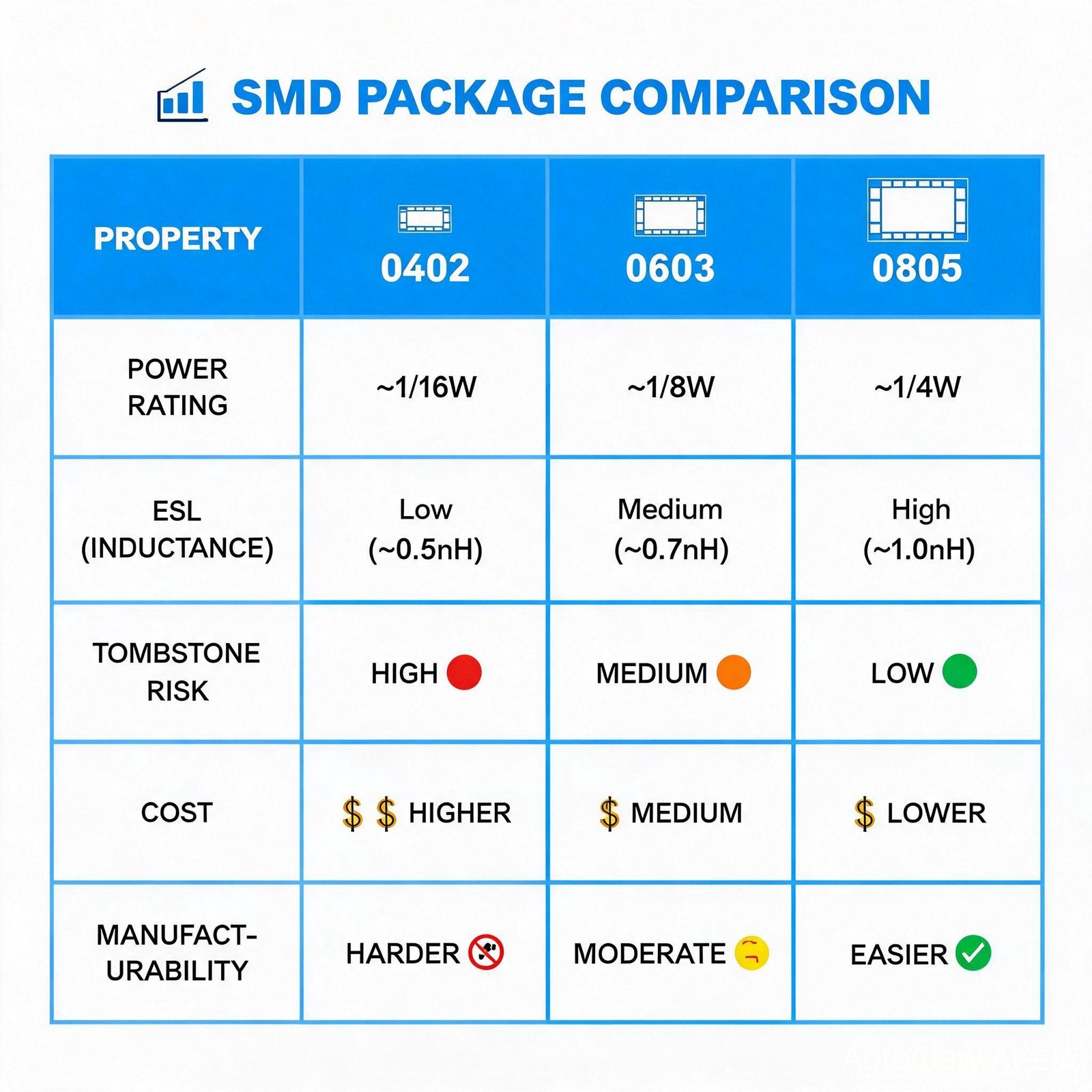
5. Comprehensive Parameter Comparison
| Parameter | 0402 (1005 Metric) | 0603 (1608 Metric) | 0805 (2012 Metric) |
|---|---|---|---|
| **Dimensions (mm)** | 1.0 × 0.5 | 1.6 × 0.8 | 2.0 × 1.2 |
| **Board Area (mm²)** | 0.5 | 1.28 | 2.4 |
| **Typical Resistor Power** | 1/16 W (0.063 W) | 1/10 W (0.1 W) | 1/8 W (0.125 W) |
| **Max Resistor Power** | 1/10 W | 1/8 W | 1/2 W (specialty) |
| **MLCC Max C (X7R)** | ~4.7 μF | ~10 μF | ~47 μF |
| **MLCC Max Voltage (typ.)** | 25–50 V | 50–100 V | 50–250 V |
| **ESL (typical)** | 0.2–0.4 nH | 0.4–0.6 nH | 0.6–0.9 nH |
| **Tombstone Risk** | Moderate (0.05–0.2%) | Low (0.01–0.05%) | Very Low (<0.01%) |
| **MLCC Flex Crack Resistance** | Best | Good | Moderate |
| **Hand-Solderable** | Difficult (microscope needed) | Feasible (with practice) | Easy |
| **Relative Cost (100k qty)** | 100% (baseline) | 70–85% | 50–70% |
| **Recommended Pad Pitch** | 0.5–0.6 mm | 0.8–1.0 mm | 1.0–1.3 mm |
| **Typical Applications** | Smartphones, wearables, RF | General-purpose, IoT, automotive | Power supplies, industrial, prototyping |
6. Application-Specific Selection Guide
6.1 Mobile & Wearable Electronics
Recommended: 0402 for decoupling and signal paths; 0201 or 01005 for extreme density.
Smartphone PCBs routinely use 0402 as the default passive package, with 0201 for bypass capacitors near BGA-packaged processors. The combination of low ESL, small footprint, and superior flex-crack resistance makes 0402 the only viable choice for thin-form-factor devices. Apple's iPhone logic boards have used 0201 and 01005 components since the iPhone 7, with 0402 relegated to non-critical locations [7].
6.2 Industrial & IoT
Recommended: 0603 across the board, with 0805 for power sections.
Industrial designs prioritize reliability, reparability, and wide temperature range over absolute miniaturization. The 0603 package offers an optimal balance: good power handling for 24 V sensor interfaces and 4–20 mA loops, reasonable hand-solderability for field repairs, and high availability from multiple suppliers. Power supply sections (DC-DC converters, relay drivers) benefit from 0805 components where voltage ratings and power dissipation are primary concerns.
6.3 Automotive Electronics
Recommended: 0603 for infotainment/body electronics; 0805 for powertrain; AEC-Q200 qualification mandatory.
Automotive applications demand AEC-Q200 qualified passives. For infotainment and ADAS processing boards, 0603 MLCCs and chip resistors are standard, with 0402 entering ADAS computer modules for high-speed decoupling. Powertrain applications (engine control units, transmission controllers) predominantly use 0805 and larger packages (1206, 1210) due to higher voltage requirements and thermal cycling stress. Automotive PCB designers must also account for the IPC-6012DA Class 3 reliability requirements, which impose stricter pad geometry rules that favor larger packages [8].
6.4 Military & Aerospace
Recommended: 0805 minimum; MIL-PRF qualified components required.
Military and aerospace designs operate under extreme environmental conditions: -55°C to +125°C (or wider), high vibration, and zero-failure-tolerance requirements. MIL-PRF-55342 (resistors) and MIL-PRF-55681 (capacitors) qualification mandates stringent testing that is rarely available below 0805. Design derating guidelines (e.g., MIL-STD-975 for NASA applications) typically require capacitors to operate at ≤50% of rated voltage and resistors at ≤50% of rated power, further pushing designers toward larger packages [9].
6.5 Prototyping & Makers
Recommended: 0805 for hand-assembly; 0603 if PCB reflow is available.
For breadboard prototyping, hobbyist projects, and university labs, 0805 remains the practical default. The components are large enough to handle with tweezers, clearly marked (resistor values are often laser-etched), and compatible with inexpensive soldering stations. 0603 is a reasonable step down if a reflow oven or hot plate is available.

7. Design Rules and Layout Best Practices
7.1 Pad Geometry
Follow IPC-7351 land pattern recommendations. Key considerations per package:
- **0402:** Pad width 0.5–0.6 mm, gap 0.4–0.5 mm. Use solder mask defined (SMD) pads for better alignment.
- **0603:** Pad width 0.8–1.0 mm, gap 0.6–0.8 mm.
- **0805:** Pad width 1.2–1.4 mm, gap 0.8–1.0 mm.
7.2 Thermal Relief
For components connected to large copper planes, use thermal relief spokes (typically 0.25–0.4 mm width) to prevent tombstoning caused by one termination cooling faster than the other during reflow. This is especially important for 0402 packages on multilayer boards with internal ground/power planes [5].
7.3 Mixed-Package Design Rules
When mixing package sizes on the same board:
- Group identical package sizes into common placement zones to simplify pick-and-place programming.
- Maintain ≥1.5 mm clearance between 0402 and tall components (connectors, electrolytic capacitors) to allow stencil printing and rework access.
- Align all passives in the same orientation (e.g., all horizontal) to improve solder joint inspection consistency via AOI (Automated Optical Inspection).
8. Future Trends: What's Next for SMD Passives
The electronics industry continues its inexorable march toward miniaturization. 0201 (imperial 0.024″ × 0.012″, or 0.6 mm × 0.3 mm) and 01005 (0.4 mm × 0.2 mm) are now standard in flagship smartphones and hearables. The 008004 package (0.25 mm × 0.125 mm) has been demonstrated for ultra-high-density applications [10].
However, the 0402–0603–0805 ecosystem is far from obsolete. The massive installed base of assembly equipment, the deep supplier catalog, and the proven reliability history of these packages ensure their continued dominance in industrial, automotive, and general-purpose designs for the foreseeable future. The emergence of advanced MLCC dielectrics (Class II X8L, X8R for high-temperature applications) also means that larger packages can achieve capacitance densities previously unattainable, preserving their relevance in power electronics.
9. References
[1] KEMET Electronics, "Surface Mount MLCC Capacitance Range by Case Size," Technical Bulletin, 2025.
[2] EIA (Electronic Industries Alliance), "EIA-198: Ceramic Dielectric Capacitors Classes I, II, III, and IV," Section 3.1: Package Nomenclature.
[3] H. W. Ott, Electromagnetic Compatibility Engineering, 2nd ed. Hoboken, NJ: Wiley, 2024, Ch. 11: "Decoupling and Bypass Capacitor Selection."
[4] IPC/JEDEC-9704A, "Printed Wiring Board Strain Gage Test Guideline," JEDEC Solid State Technology Association, 2012.
[5] J. S. Hwang, "Minimizing Tombstoning Defects in Chip Component Assembly," SMT Magazine, vol. 38, no. 4, pp. 22–29, 2024.
[6] Vishay Intertechnology, "D/CRCW e3 Series: Standard Thick Film Chip Resistors," Datasheet, Rev. 2025.
[7] TechInsights, "iPhone 16 Pro Max Teardown: Component Package Analysis," 2025.
[8] IPC-6012DA, "Automotive Applications Addendum to IPC-6012D," IPC International, 2020.
[9] NASA, "MIL-STD-975L: NASA Standard Electrical, Electronic, and Electromechanical (EEE) Parts List," Revision L, Section 4.2: Derating Guidelines.
[10] Murata Manufacturing, "008004-inch Size Multilayer Ceramic Capacitor: GRM011 Series," Product Introduction Note, 2025.
External Links:
- KEMET SMD MLCC Selection Guide: `https://www.kemet.com/en/us/technical-resources.html`
- IPC-7351 Land Pattern Calculator: `https://www.pcb.com/resources/ipc-7351`
- Vishay Resistor Product Selector: `https://www.vishay.com/resistors/`
- Murata SimSurfing (MLCC Characteristics): `https://ds.murata.co.jp/simsurfing/mlcc.html`
- JEDEC Publication JEP95: Package Registration: `https://www.jedec.org/standards-documents`
FAQ
Q1: Can I mix 0402, 0603, and 0805 passives on the same PCB?
Absolutely. Most production PCBs use multiple package sizes. Decoupling capacitors near high-speed ICs may be 0402 for low ESL, while bulk capacitors and power resistors remain 0603 or 0805. Ensure your assembly house supports all package sizes in your BOM, and follow mixed-package layout best practices (Section 7.3).
Q2: Is 0603 or 0402 better for a general-purpose IoT PCB?
0603 is generally the better choice for general-purpose IoT designs. It offers adequate power handling for sensor interfaces and wireless modules, lower cost than 0402, and easier prototyping. Reserve 0402 for high-density sections where board space is critical (e.g., directly beneath a BGA-packaged wireless SoC).
Q3: Why do some 0402 MLCCs crack less than 0805 under board flex?
This is due to mechanical leverage. Board flexing generates a bending moment that is distributed across the component body. A shorter 0402 body (1.0 mm) experiences less total strain per unit length than a longer 0805 body (2.0 mm). This is quantified in IPC/JEDEC-9704 testing — 0402 components consistently survive higher board strains before cracking [4].
Q4: What tombstoning prevention measures are most effective for 0402?
Key measures include: (1) symmetrical pad geometry with identical dimensions and thermal connections for both terminations, (2) thermal relief spokes on pads connected to large copper planes, (3) nitrogen-atmosphere reflow for consistent solder wetting, (4) optimized stencil aperture design (typically 1:1 aspect ratio with rounded corners), and (5) controlled ramp rate during preheat (1–2°C/second) [5].
Q5: When should I choose an 0805 resistor over a 0603 resistor?
Choose 0805 when: (a) power dissipation exceeds 0.1 W (0603 max); (b) you need higher voltage handling for divider or sense circuits; (c) the design will be hand-assembled without reflow equipment; (d) the resistor is in a high-current path (current sensing, LED drivers); or (e) the application requires through-hole-alternative components for visual inspection in legacy repair workflows.
Q6: How does package size affect PDN (Power Distribution Network) impedance?
Package size affects PDN impedance primarily through ESL. Lower ESL (0402) shifts the capacitor's self-resonant frequency (SRF) higher, providing effective decoupling at higher frequencies. For a typical PDN targeting 10 mΩ impedance from DC to 100 MHz, 0402 capacitors are preferred for the high-frequency decoupling tier (≥10 MHz), 0603 for mid-frequency, and 0805 or larger (tantalum, aluminum polymer) for bulk decoupling (<1 MHz) [3].
